Essential Daifuku Technologies for Social InfrastructureImproving Reliability and Productivity with Daifuku’s Semiconductor Production Line Systems
When it comes to semiconductor manufacturing, highly reliable transport and storage systems capable of operating 24 hours a day, 365 days a year are essential. We spoke with engineering and design staff representatives from Daifuku’s Cleanroom Division about Daifuku’s semiconductor production line systems such as the Cleanway, a cleanroom transport system for maximizing equipment uptime, and a nitrogen purge storage system that contributes to semiconductor miniaturization.
Trends in semiconductor fabrication plants: Consolidation and increased scale
Semiconductors are an essential component used in many everyday electronic devices such as computers and smartphones. They are also an important part of growing fields such as automated driving technology, electric vehicles (EVs), and artificial intelligence (AI). Semiconductor manufacturers around the world are having to increase their production capacities to keep up with the growing demand. Governments across the globe have announced policies to subsidize intra-regional investment, paving the way for continued strong capital investment by manufacturers.
To better meet the increased demand, many major players in the industry are consolidating and increasing the scale of their production facilities. Having semiconductor fabrication plants (fabs) located close together rather than dispersed across several different locations helps reduce construction costs and saves resources during manufacturing. Consolidation is also good for operating expensive state-of-the-art equipment by making it easier for such equipment to be shared by different plants.
With these industry trends in mind, the Daifuku Group offers various solutions for ensuring not only smooth transportation within a fab, but also efficient transportation of semiconductor wafers between connected fabs.
Example solutions for the increased scale of consolidated semiconductor fabs
Daifuku systems for front-end and back-end processes
Semiconductors are manufactured in a cleanroom environment where dust and other airborne particles are strictly controlled. Raw silicon material is first melted down to make an ingot. This ingot is thinly sliced into uniform wafers. Current mainstream wafers are cut into a disk-shape with a diameter of 300 mm. The wafer then undergoes the processes of photolithography and etching dozens of times to imprint integrated circuits onto the surface. This is referred to as front-end processing. The following processes of cutting the chips from the wafer and converting them into CPUs and other products are referred to as back-end processing.
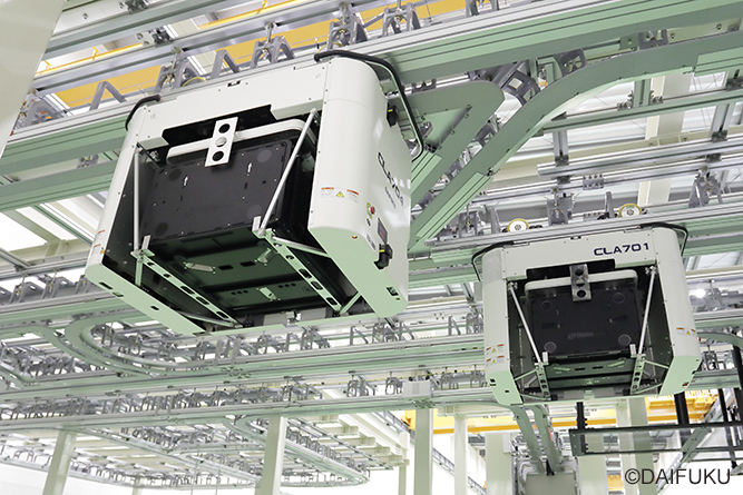
Daifuku offers semiconductor manufacturing conveyance for both front-end and back-end processing through Cleanway, a cleanroom conveyance system that uses electrically powered vehicles. In front-end processing, wafers are stored in a sealed container called a FOUP to keep them clean while they are being moved between various processing equipment. Daifuku’s Cleanway system transfers all FOUPs between the equipment automatically. Because the Cleanway system’s transport rails are stretched across the ceiling rather than laid out on the floor, there is space to install numerous other devices in the cleanroom, making it a popular choice in many semiconductor fabs. The materials used in the wheels of the vehicle have also been carefully designed to minimize the generation of dust.
The Clean Stocker is a temporary storage device used together with the Cleanway system. Although front-end processing tasks are performed repeatedly, the time required for each operation varies. FOUPs containing wafers waiting to be sent to the next process are stored in a stable temporary storage device called a stocker. As manufacturing periods become longer and semiconductors become smaller, it is becoming increasingly common to fill the FOUP with nitrogen gas to prevent oxidation. Daifuku provides systems with nitrogen purge capabilities to meet this growing need.
Semiconductor production line system with nitrogen purge stocker
Although the bulk FOUP storage provided by stockers is helpful, they are often located away from the transfer route, and in some fab layouts, getting to and from the stocker can take some time. Side track buffers (STBs)—receiving platforms installed in the open space between transport rails—are becoming a popular solution to this problem. In some cases, using STBs can shorten the 180-day manufacturing time of the latest CPUs by about 5 days. While a 5-day reduction on a 180-day manufacturing schedule may not seem like much at first glance, a constant 3% reduction in delivery time is a significant achievement for any semiconductor factory looking to increase efficiency and productivity.
Using STBs also helps contribute to sustainability. Whereas installing stockers requires a certain amount of floor space, STBs use platforms hung from the ceiling, helping to save cleanroom space for other equipment and thus reducing the overall footprint of the facility. For these reasons, STBs are becoming a popular method for saving energy and improving efficiency.
Directing traffic with AI
As semiconductor factories continue to grow larger in scale, the total length of Cleanway rails can reach combined lengths of over 200 km with more than 10,000 vehicles operating on them. Although the wafer processing procedures have a fixed order, the time it takes to complete each one can vary greatly, and this can lead to traffic jams as vehicles become concentrated around certain equipment at certain times. These traffic jams limit productivity, and Daifuku has begun using AI in the Cleanway system control software to prevent such jams from occurring. Just as with in-car navigation systems, AI is used to determine a route that avoids traffic congestion, with each vehicle being directed to its optimal route. Whereas conventional systems select the route according to the shortest distance, the adoption of AI makes it possible to dynamically determine and select the quickest route possible, even if that route is actually a longer distance. The anticipated advancements in AI technology mean it has great potential for further improving systems and Daifuku will continue to explore its use.
Improving semiconductor manufacturing through advanced control technology
Operating a large-scale facility 24 hours a day, 365 days a year, is no easy task, so Daifuku is dedicated not only to offering durable hardware that can withstand long-term use, but also to developing auxiliary systems and providing redundancy to support stable and smooth fab operation.
For example, the Cleanway system adopts the HID non-contact power supply system to minimize the generation of dust that would be caused by the abrasion of a contact power supply. The HID system also incorporates redundancy measures to ensure a continuous supply of power to the vehicles. Essential system operation components such as controllers and servers are also prepared in duplicate, ensuring continued operation even if a device malfunctions.
In addition, whereas controllers were previously installed at rail junctions to prevent vehicle collisions, the current system uses wireless control, eliminating the need to place control equipment. Information is shared wirelessly between vehicles approaching a junction, and only after determining that the vehicles will not collide with each other are they allowed to proceed. By reducing the amount of equipment installed on the rails, the system costs less, is quicker to install, and uses less material and energy, making it more environmentally friendly.
Meeting automation needs in back-end processes
In recent years, there has been a growing need for automation in the back-end processes of semiconductor manufacturing. While previously it was common to make productivity improvements through advances in front-end processes, advances in back-end processes, such as wafer cutting and chip packaging, are also essential for improving efficiency in fabs. Compared with front-end processes, back-end processes rely more heavily on manual labor, including the transport of the chips, and frequently take place outside of a cleanroom, so by moving to a controlled clean environment and automating transfers between processes, fabs are able to produce higher-quality products with increased efficiency.
Support for rectangular-shaped wafers is also a growing need. In current front-end processes, circuits are commonly baked into circular silicon wafers, but because the wafers end up being cut into square chips in back-end processing, the wafers do not necessarily need to be circular. As such, using square packages more similar to the end-product is becoming a popular way to prevent waste in back-end processes.
Utilizing technology cultivated in the transportation of OLED panels, Daifuku has developed FOUP transport systems for panel-level packages (PLPs) capable of handling 600 mm square substrates. Through adapting to square substrates and other system improvements, Daifuku solutions provide even further benefits to semiconductor fab efficiency.
Back-end processing solutions for semiconductor manufacturing
Utilizing offices around the world for localized responses
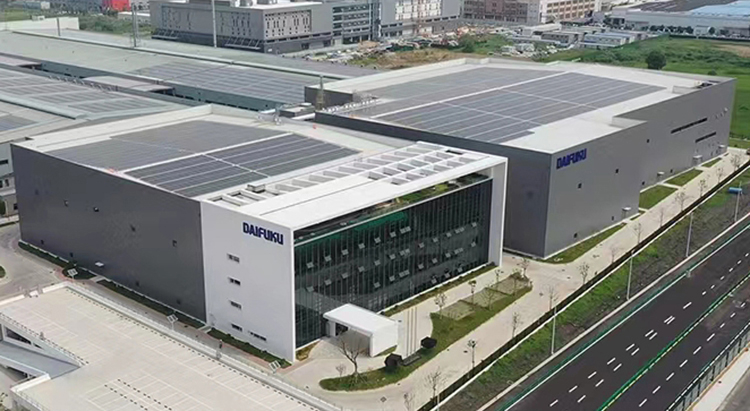
In addition to Shiga Works, Daifuku’s flagship manufacturing plant, the Cleanroom Global Business also has production plants in China, Taiwan, and South Korea as well as subsidiaries in the US and Singapore. Although the core components of the equipment are sent from Japan, the transport rails and other components are designed and assembled in local factories. This is commonly referred to as “local production for local consumption.” Local subsidiaries employ not only sales representatives but also engineers, allowing for more detailed communication with customers. This makes it possible for engineers to work directly with customers, including responding to requests and feedback, without the need for onsite visits by staff from Japan. This unique ability to respond immediately to customers is one of the Daifuku Group’s greatest strengths, and it makes it possible to incorporate feedback from users around the world into the design and development of products.
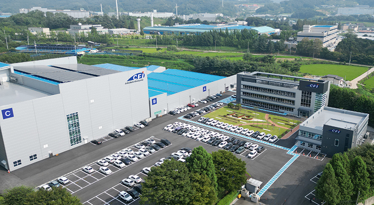
Production sites in China (left) and South Korea (right)
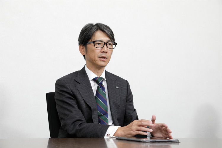
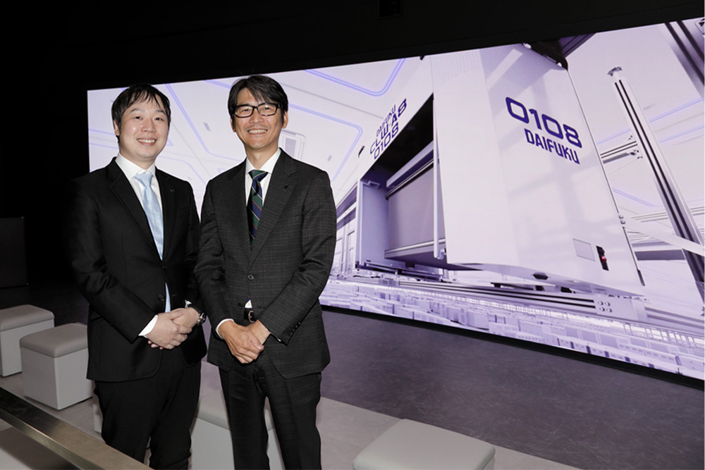
Shinichi Nakashima
Manager, Engineering Department, Sales Operations, Cleanroom Division
Daifuku Co., Ltd.
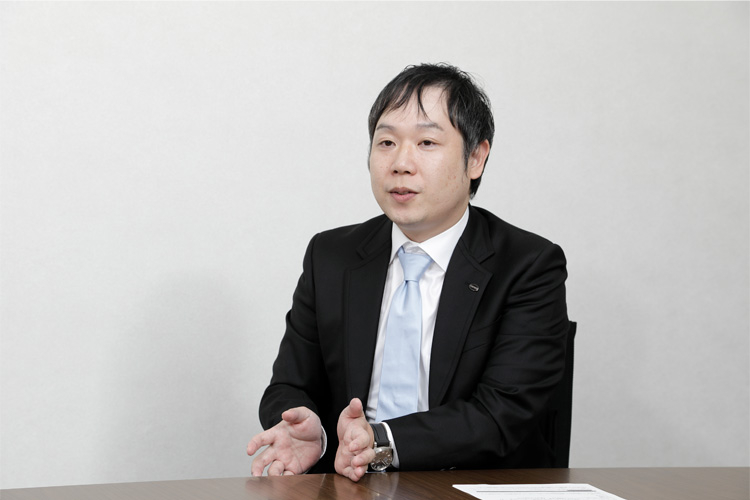
Tatsuki Ii
Assistant Manager, VHL Design Section 2
Transport Design Group, Design Department, Production Operations, Cleanroom Division
Daifuku Co., Ltd.